Electronics Thermoforming Packaging Manufacturer IndiaESD-Safe, Antistatic, Bulk from Vapi Gujarat
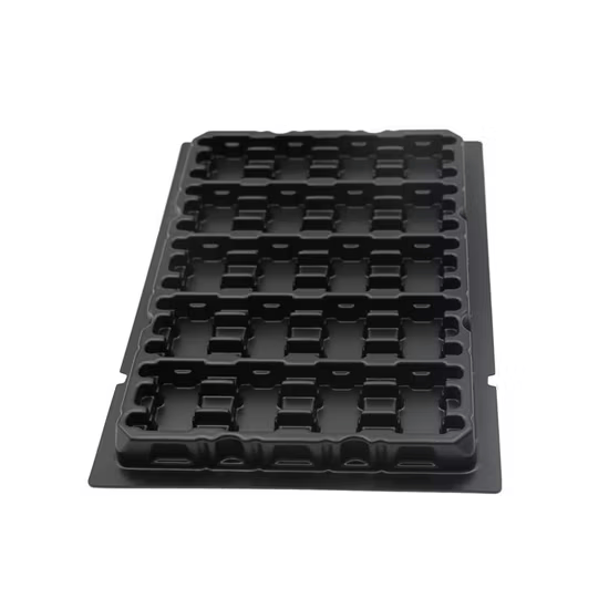
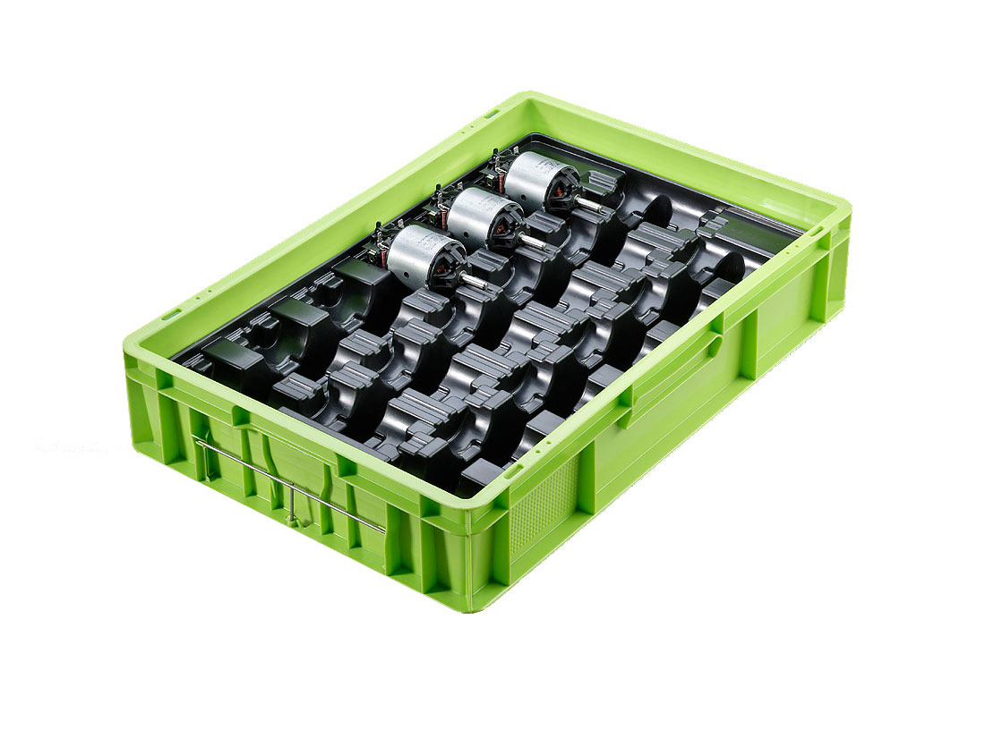
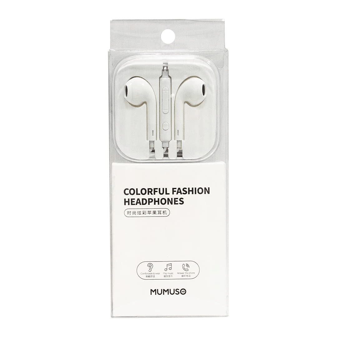
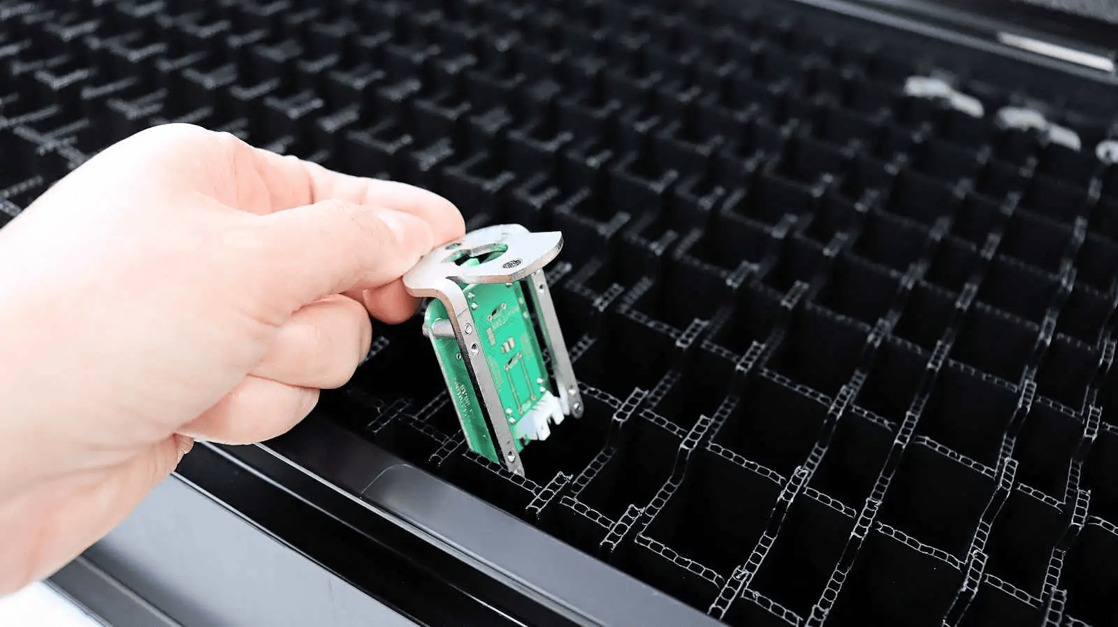
Custom ESD-safe thermoformed electronics packaging for the complete electrical and electronic component range — ESD-safe thermoforming trays, PCB and circuit board packaging, connector and micro-component trays, consumer electronics accessory packaging, and switches and sensor module packaging. ESD packaging OEM from Vapi Daman — ISO 9001:2015, resistivity CoA per batch.
Electronics Thermoforming Packaging5 Sub-Categories, ESD-Safe, Bulk OEM from Vapi
Trizen Packaging manufactures electronics thermoforming packaging from our ISO 9001:2015 certified facility in Vapi, Gujarat — ESD-safe thermoformed packaging for the complete electrical and electronic component range. ESD packaging OEM from Vapi Daman for ESD-safe thermoforming trays, PCB and circuit board packaging, connector and micro-component trays, consumer electronics accessory packaging, and switches, sensors, and electronic module packaging. With 20+ years of thermoforming manufacturing experience, we are an electronics thermoforming packaging manufacturer from India serving electronics manufacturers, EMS companies, and OEMs across India and for export.
Electronics packaging requires one critical capability that standard thermoforming cannot provide: ESD (electrostatic discharge) protection. Electronic components can sustain permanent damage from ESD at voltages as low as 10–30 volts — completely imperceptible levels that cause latent damage passing visual inspection but manifesting as field failure in service. Standard PP thermoforming materials are insulators — they generate and accumulate electrostatic charge. ESD-safe PP and ESD-safe PETG have controlled surface resistivity in the dissipative range (10⁶–10⁹ Ω/sq) that dissipates charge rather than accumulating it.
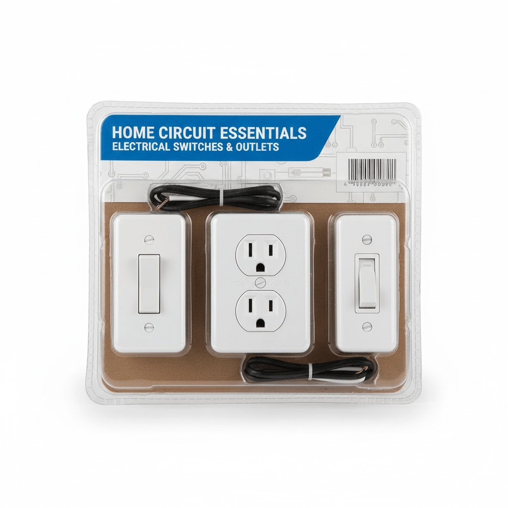
Electronics Packaging OEM — ESD-Safe, Bulk from Vapi
ESD-safe PP & PETG · Resistivity CoA per batch · ISO 9001:2015 · 7–14 day prototype.
Why Electronics Thermoforming Packaging Is Technically Demanding
Three Problems Electronics Packaging Buyers Face
Electronics Packaging — ESD-Safe OEM from Vapi
ESD-safe PP & PETG · Resistivity CoA per batch · 7–14 day prototype · ISO 9001:2015.
Materials for Electronics Thermoforming Packaging
| Material | Electronics Application | Surface Resistivity | Key Property |
|---|---|---|---|
| ESD-Safe PP | Primary ESD electronics packaging — PCB trays, connector trays, sensor packaging, module packaging | 10⁶–10⁹ Ω/sq (dissipative) | ESD charge dissipation, rigid geometry, cost-efficient OEM volumes |
| ESD-Safe PETG | Precision electronics requiring optical clarity — inspection through packaging, ADAS sensors, optoelectronics | 10⁶–10⁹ Ω/sq (dissipative) | ESD protection + crystal clarity for visual inspection before use |
| APET (Crystal-Clear) | Consumer electronics retail packaging — where ESD risk is low (accessories, cables, non-sensitive items) | Insulating range (not ESD-safe) | Crystal clarity, tamper-evident, retail shelf presence |
| PP (Standard) | Non-ESD-sensitive electronics outer packaging only — never in contact with ESD-sensitive components | Insulating range (not ESD-safe) | Standard thermoforming — do not use for ESD-sensitive component packaging |
Why Electronics Manufacturers Choose Trizen Packaging
Frequently Asked QuestionsElectronics thermoforming packaging
Custom ESD-safe thermoformed packaging for the complete electronics range: ESD-safe thermoforming trays, PCB and circuit board packaging, connector and micro-component trays, consumer electronics accessory packaging, and switches, sensors, and electronic module packaging. ESD-safe PP and PETG with surface resistivity CoA per batch. ISO 9001:2015. ESD packaging OEM from Vapi, Gujarat.
ESD-safe thermoforming uses materials with controlled surface resistivity in the dissipative range — typically 10⁶ to 10⁹ Ω/sq — that continuously dissipate electrostatic charge rather than allowing it to accumulate and discharge through electronic components. Electronic components can sustain permanent ESD damage at as low as 10 to 30 volts — imperceptible to human senses but permanently damaging to semiconductor devices. ESD-safe packaging eliminates the charge accumulation mechanism.
Dissipative range: 10⁶ to 10⁹ Ω/sq for ESD-safe PP and ESD-safe PETG. This range dissipates charge slowly enough to prevent rapid discharge current through components while preventing accumulation to damaging charge levels. Surface resistivity confirmed per material batch by CoA. Available for OEM and EMS supplier qualification review.
ESD-safe PP (primary — PCB trays, connector trays, sensor packaging, module packaging, dissipative range), ESD-safe PETG (precision electronics requiring optical clarity through packaging), APET crystal-clear (consumer electronics retail packaging for non-ESD-sensitive accessories). See PETG materials page.
ESD packaging OEM manufacturer Vapi Daman — all ESD-safe electronics packaging tooling in-house at our Vapi, Gujarat facility. Electronic component thermoforming manufacturer Gujarat serving electronics manufacturers and EMS companies across India. As an electronics packaging manufacturer from India, also serving export electronics manufacturing programmes.
Standard PP surface resistivity is in the insulating range (>10¹² Ω/sq) — it generates and holds electrostatic charge, creating the risk of damaging ESD discharge to enclosed components. ESD-safe PP surface resistivity is in the dissipative range (10⁶–10⁹ Ω/sq) — charge is continuously dissipated. The visual difference between ESD-safe and standard PP is minimal — the functional difference is complete ESD protection vs no ESD protection.
Prototype: 7 to 14 business days from component sample or technical drawing — in-house CNC tooling at Vapi. MOQ from 500 units. Sustained OEM from 5,000 units per run. ESD material CoA and ISO 9001:2015 batch documentation per production run.
Electronics Thermoforming Packaging — ESD-Safe OEM from Vapi
ESD-safe trays · PCB packaging · Connector trays · Sensor packaging · Consumer electronicsESD-safe PP & PETG · Resistivity CoA per batch · ISO 9001:2015 · Vapi, Gujarat