PCB & Circuit Board Packaging Manufacturer IndiaESD-Safe Antistatic PCB Trays, Bulk from Vapi
Custom ESD-safe antistatic thermoformed trays for PCBs and circuit boards — bare PCB packaging, assembled board trays, gold finger edge connector protection, component height clearance. Bulk PCB packaging trays from Vapi — ESD-safe PP, antistatic PCB tray supplier Gujarat, ISO 9001:2015.
 Click for
full photo
Click for
full photo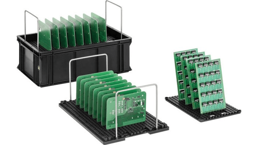 Click for
full photo
Click for
full photo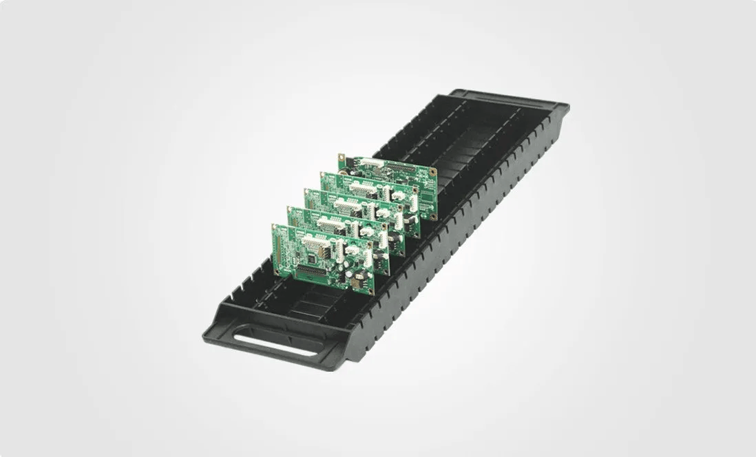 Click for full
photo
Click for full
photoPCB & Circuit Board Packaging Manufacturer IndiaESD-Safe Antistatic PCB Trays, Bulk from Vapi
Trizen Packaging manufactures PCB and circuit board packaging from our ISO 9001:2015 certified facility in Vapi, Gujarat — custom ESD-safe antistatic thermoformed trays for bare PCBs, assembled circuit boards, and mixed-technology boards. Bulk PCB packaging trays from Vapi for PCB manufacturers, EMS companies, electronics OEMs, and PCB distributors across India and for export. As a PCB circuit board packaging manufacturer from India, we supply ESD-safe antistatic packaging for domestic electronics manufacturing and export PCB supply chains.
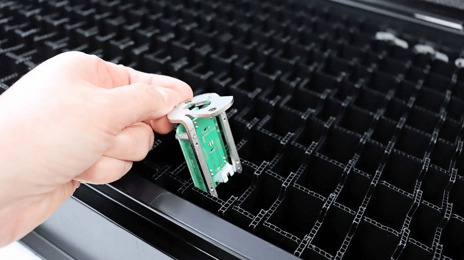
PCB packaging has two critical design dimensions that no other electronics packaging application requires simultaneously: gold finger protection and component height clearance. Gold fingers (exposed edge connector pads at the PCB perimeter used for PCB-to-PCB connection) must not contact any packaging material — contamination or mechanical damage to gold finger pads causes connector failure. Component height — the maximum height of any component on the assembled PCB — determines the minimum cavity height the packaging must provide without component contact.
| Device / Component | Packaging Format | Material | Key Requirement |
|---|---|---|---|
| Bare PCBs (Single & Double Layer) | Multi-PCB ESD-safe PP tray — PCBs stacked with separator | ESD-safe PP | Gold finger edge clearance, PCB surface no-contact, ESD-safe |
| Multilayer PCBs | Individual cavity ESD-safe PP tray | ESD-safe PP | Edge connector protection, via exposure, PCB warp prevention under stack |
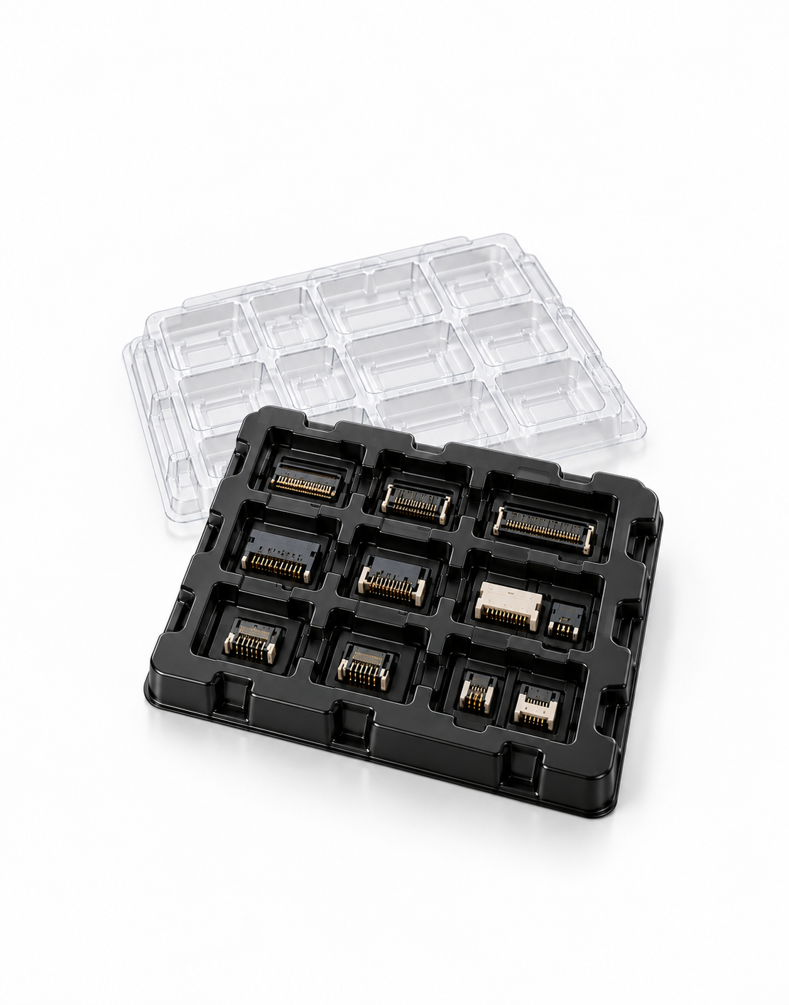
| Assembled PCBs (SMT populated) | Cavity tray with component height clearance | ESD-safe PP | All components clear of cavity ceiling, gold finger edge clearance, ESD-safe |
| High-Power PCBs & Heatsink Assemblies | HDPE or ESD-safe PP heavy-duty tray | ESD-safe PP or HDPE | Heatsink geometry clearance, heavy assembly support, thermal pad protection |
| Flexible PCBs & FPCs | ESD-safe PETG tray — FPC in flat position | ESD-safe PETG | FPC flat geometry preservation, connector tab protection, ESD-safe |
| PCB Sub-Assemblies | Multi-component ESD-safe PP tray | ESD-safe PP | All sub-assembly components organized, connector protection, ESD-safe |
| PCB OEM Bulk Supply | High-density ESD-safe PP bulk supply tray | ESD-safe PP | Maximum PCB count per tray, ESD-safe throughout supply chain |
PCB & Circuit Board Packaging — ESD-Safe OEM from Vapi
ESD-safe PP & PETG · Resistivity CoA per batch · ISO 9001:2015 · 7–14 day prototype.
Three Problems PCB & Circuit Board Packaging Buyers Face
PCB & Circuit Board Packaging Key Design Requirements
 Click for full photo
01 / PCB control
Gold Finger Clearance Zone — No Packaging Contact on Edge Connector
The gold finger edge connector area (typically 2–5mm at the PCB perimeter) is mapped from the PCB specification before cavity design. The cavity provides a defined clearance zone over the gold finger area — no packaging material contact with the gold finger surface. Clearance width confirmed from the edge connector specification.
PCB & Circuit Board Packaging — Submit Component Sample
ESD-safe CoA · Precision cavity · 7–14 day prototype · ISO 9001:2015.
Materials for PCB & Circuit Board Packaging
| Material | Electronics Application | Key Property |
|---|---|---|
| ESD-Safe PP | Primary — all bare PCB and assembled PCB packaging | 10⁶–10⁹ Ω/sq, rigid geometry, flat PCB support, gold finger clearance compatible |
| ESD-Safe PETG | FPCs and flexible circuits requiring inspection through packaging | ESD protection + crystal clarity, FPC flat geometry |
| HDPE | Heavy PCB sub-assemblies with heatsink — weight and stack load management | Heavy-duty, maintains geometry under assembly weight and pallet stack |
Why Electronics Manufacturers Choose Trizen for PCB & Circuit Board Packaging
Frequently Asked QuestionsElectronics thermoforming packaging
Custom ESD-safe antistatic thermoformed trays for bare PCBs, multilayer PCBs, assembled PCBs, high-power PCB assemblies, flexible PCBs, PCB sub-assemblies, and PCB OEM bulk supply. ESD-safe PP and PETG. ISO 9001:2015. Bulk PCB packaging trays from Vapi, Gujarat.
Gold fingers are exposed edge connector pads at the PCB perimeter. Gold finger contamination from packaging material contact causes contact resistance failures. Gold finger clearance zone in the cavity — no packaging material contact with the gold finger surface. Clearance confirmed from PCB specification before tooling.
Maximum height of any populated component confirmed from PCB assembly drawing or physical measurement. Cavity height designed for minimum 2mm clearance above maximum component height under pallet stack load.
Bare PCB substrate is ESD-sensitive. Assembled PCB populated components are ESD-sensitive. ESD-safe PP for both applications — CoA per batch confirms dissipative range.
Bulk PCB packaging trays Vapi. PCB packaging manufacturer Gujarat. Antistatic PCB tray supplier Gujarat. ISO 9001:2015 and ESD CoA per run.
ESD-safe PP: 10⁶–10⁹ Ω/sq dissipative range. Confirmed by surface resistivity CoA per material batch. Compliant with ANSI/ESD S541 and IEC 61340-5 requirements — confirm specific standard at brief stage.
Prototype: 7 to 14 business days from PCB sample or drawing. MOQ from 500 units. ESD CoA and ISO 9001:2015 per batch.
PCB & Circuit Board Packaging — ESD-Safe OEM from Vapi
ESD-safe PP & PETG · Resistivity CoA per batch · ISO 9001:2015 · 7–14 day prototype · Vapi, Gujarat